Disclaimers: DC to DC Boost ConverterThere are many different switching voltage regulator topologies like buck, boost, buck-boost, and chuck. However, this paper covers the design and construction of a boost converter only. This converter is capable of boosting a 12V input voltage to a variable 12 to 24V output voltage (potentiometer controlled). The boost converter steps-up the input voltage by storing the electrical energy in an inductor and then releasing this energy to the load at a higher voltage level.
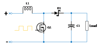
Boost Converter (Variable 12 to 24V output)
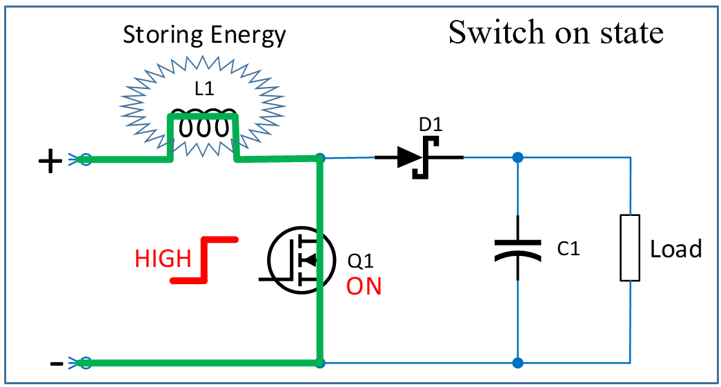
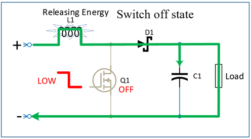
The main working principle of the boost converter is that when the MOSFET is on, the inductor stores energy in the form of magnetic energy and discharges it when the MOSFET is open as shown in the figures below.
Objectives:
The objective of this project is to design and analyze a boost converter circuit that is capable of boosting a 12V input into a variable 12V to 24V output. This tutorial will introduce an approach to design a boost converter using the MAX1771 step-up switching controller IC as a gate driver and controller. We will also design and fabricate a printed circuit board (PCB) and a 3D printed enclosure as a prototype design.
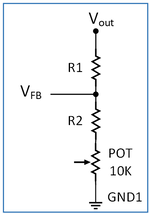
To find the calculated output voltage, we have to use the following formula from the MAX1771 datasheet.
\(\color{blue}{V_{out} = V_{RF}*(\frac {R_{1}} {{R_{2}+R{pot}}})+1}\) 2- Duty Cycle calculation:
The duty cycle is calculated using the following formula. \(\color{blue}{D = 1+ (\frac {(V_{IN}) * (Eff_{GD})} {V_{OUT}})}\) 3- Inductor calculation
Before we calculate the inductor value, we have to take the recommended estimation of inductor ripple current in the datasheet that is from 20% to 40% of the output current. Our maximum expected current is 1A, and let's use 40% ripple current (worst case scenario). Similarly, the maximum frequency is obtained from the datasheet that is 300kHz. Using this information, the inductor value is calculated as follows. \(\color{blue}{L = (V_{IN} *\frac {(V_{OUT}) - (V_{IN})} {(f_s * DI_L*V_out)})}\) 4- Output Capacitor calculation
In order to calculate the value of the output capacitor, first we need to determine the expected output ripple voltage. Set the desired output voltage ripple to be 1% as per the recommendation from the MAX1771 datasheet. Then, the output capacitor is calculated using the following formula. \(\color{blue}{C_{out_{min}} = (\frac {(I_{OUT_max}) * (D)} {(f_s * DV_out)})}\) The frequency of the MAX1771 is obtained from the datasheet (300kHz), the maximum required current for our boost converter is 1A. Then, using these values, the minimum capacitor value is determined as follows:
\(\color{blue}{C_{out_{min}} = (\frac {(1A) * (0.55)} {(300KHz * 0.1V)})= 18.33uF}\) Circuit diagram
For this design, The MAX 1771 gate driver and controller is the main component. According to the datasheet, “The MAX1771 step-up switching controller provides 90% efficiency over a 30mA to 2A load.” This gate driver is an 8-pin Dual in-line (DIP) IC that is smaller in size and it greatly reduces PCB board space. The input voltage ranges from 2V – 16V but it is best at 3.3 and 5V external voltage source. The gate driver furnishes up to 300KHz that is set by the controller and it has pre-set 12V output or Adjustable using a voltage divider resistor tapped into the gate driver feedback pin. Then, we can select appropriate values of the components based on the calculation above.
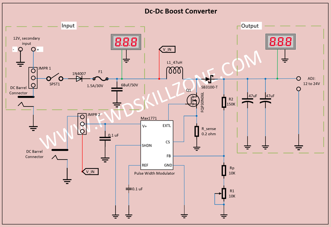
Boost converter
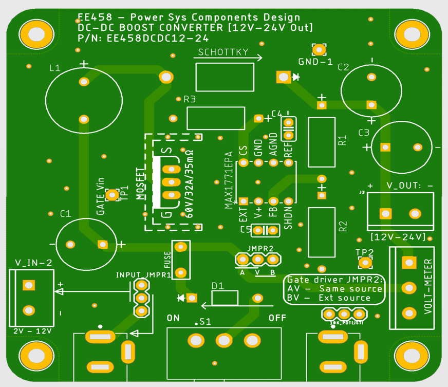
The design of the boost converter has three main section: Input, Boost, and output sections.
Input section The input section contains primary and secondary input ports selected by the jumper, “JMPR1”. It also contains single pole single throw switch, reverse current protection diode, safety fuse, input filter capacitor, and input voltage display capable of measuring 0-99V. Boost section The boost section contains jumper selected input port for the gate driver to use either the same input voltage as the boost circuit or external input DC barrel jack. The gate driver input selection is done through JMPR2. The boost section has also an input filtering capacitor, a gate driver, N-channel enhancement mode MOSFET, inductor, Schottky diode, voltage divider resistors, current sensing resistor, and a potentiometer. Output section The output section contains output filter capacitors, output port, and output voltage display. The voltage meter display used in this project is capable measuring from 0V to 99.9VDC with 0.1V precision and draws very small current of 3-4mA. Due to these characteristics, this voltage meter display is ideal for this project. The boost converter output is fed to two stripped wires connected to the output terminals. The complete circuit design is shown in the figure above. Analysis:
To analyze the boost converter, we can use the Matlab Simulink program to simulate the different stages of the converter circuit as shown in the figure below. The input voltage to the boost converter is set to 12V and varying load values are used to test the characteristics of the converter. 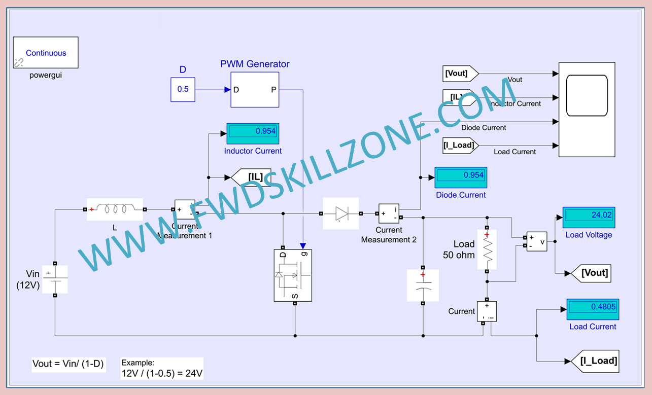
Boost converter Simulink simulation
After setting all the desired values for each component in the circuit, we set the simulation time 0.05 seconds and run the simulation. As it is shown in the waveform below, the output voltage spikes to 34.9V for few seconds and then stabilizes at 24V which is our desired output voltage. Similarly, the load current spikes 2.2A and then stabilizes at 0.44A as shown in the figure below.
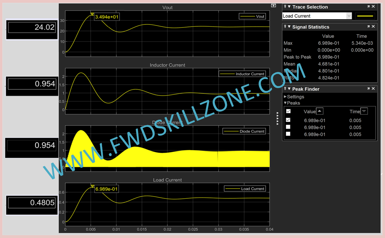
Simulink simulation output
PCB and Enclosure Design- Printed Circuit Board (PCB)
The PCB can be designed in Eagle CAD program, which can be downloaded from Autodesk website with student log in. The program helps the designer to connect schematic diagrams, component layout, PCB circuit routing, and use of component library. The free version of Eagle CAD has a limitation of only two schematic sheets, double layers, and an 80-cm2 board area. The PCB design is started in “schematic” view and all the symbols for the components are placed and oriented on a blank schematic sheet as shown in figure below. 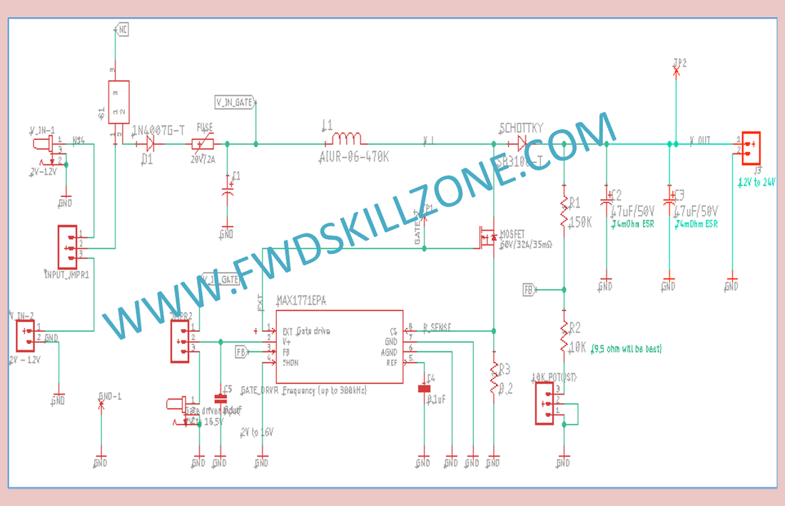
Eagle CAD schematics drawing
Next, electrical connectivity is made between each part with nets layer and assigned values and names to our parts. Finally, make sure everything is connected as per the design by running an Electrical Rule Check (ERC). Once the schematic is completed, switch to the “board” page and position the components into their actual placement. Then use “PCB Trace Width Calculator” tool to calculate the race width and route the corresponding wires with appropriate trace width of 55 mil. Then, create a copper pour of ground plane on both top & bottom layers of the PCB and connect these ground planes with multiple “Vias” to deliver heat to the opposite layer of the board and to highly reduce heat resistance.
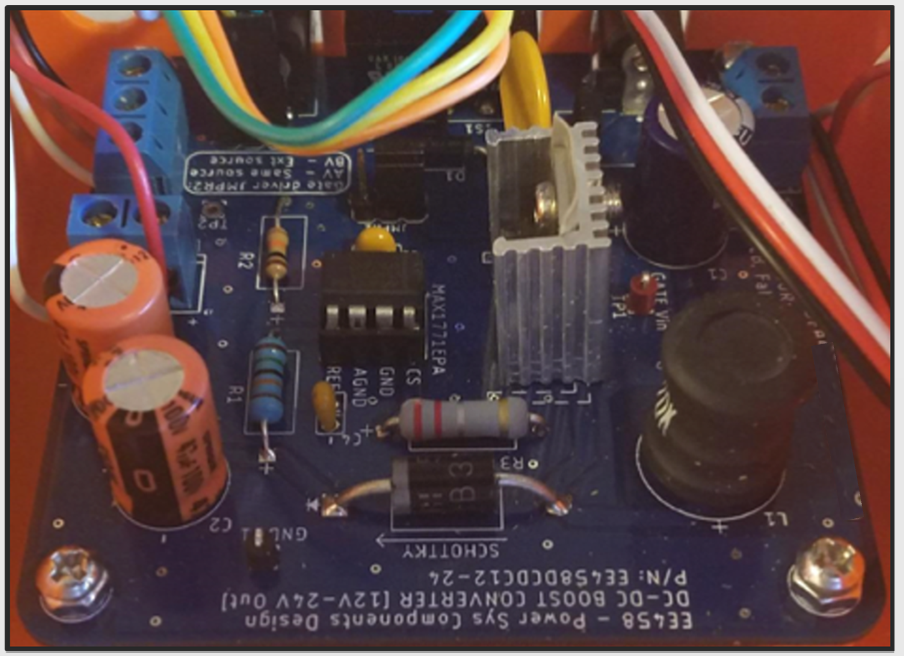
Once the PCB is fabricated, all the components are soldered onto the PCB as shown in the figure below.
The enclosure can be designed in Solid Works or any 3d designing tool. The case dimension is 125 x 100 x 64.5 mm. Once the case design is completed, the 3D model should be converted to a .stl file format for 3D printing. For this project, ABS M30 (Acrylonitrile Butadiene Styrene), Orange color material is used for the 3D printing. ABS is c0mmonly used, and most versatile materials available in 3D printing and it is strong and heat resistant comparing to other similar plastic materials. The final 3D printed case is shown in the figure below.
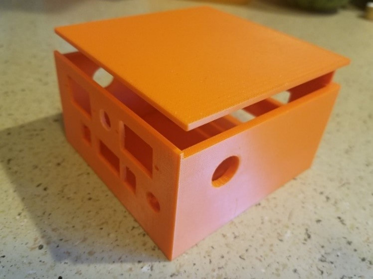
Boost converter enclosure
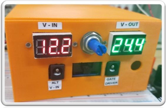
Output TestThe output test is performed by setting the potentiometer of the boost converter to the highest voltage output and by connecting two loads in parallel (a dc motor and computer fan rated from 12V to 24V). At this point, the boost converter is able to provide an output voltage of 17.8V to the load. The same setting provides 24.4V output at no load as shown in the figure below.
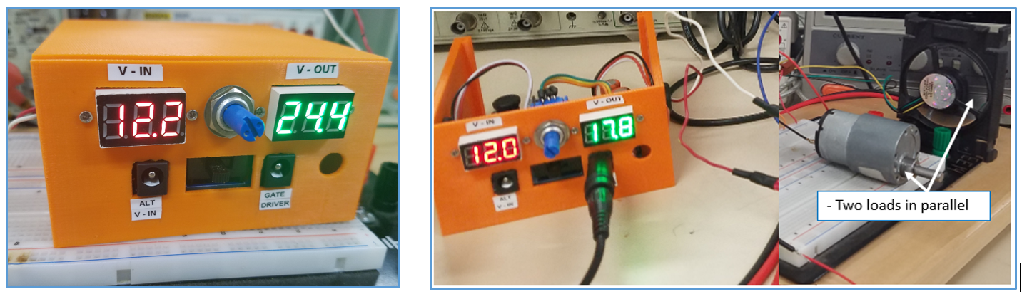
No load output (left) and full load output (right) at the maximum output potentiometer setting
»»» END of Boost Converter Design »»» Have a question or comments?
- click here to contact us |
|
|
|
|